
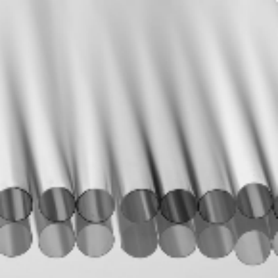
1. Crystal Structure and Polytypism of Silicon Carbide
1.1 Cubic and Hexagonal Polytypes: From 3C to 6H and Past
(Silicon Carbide Ceramics)
Silicon carbide (SiC) is a covalently bound ceramic composed of silicon and carbon atoms prepared in a tetrahedral sychronisation, creating among one of the most complicated systems of polytypism in materials scientific research.
Unlike the majority of ceramics with a single steady crystal framework, SiC exists in over 250 well-known polytypes– distinct piling series of close-packed Si-C bilayers along the c-axis– varying from cubic 3C-SiC (likewise known as β-SiC) to hexagonal 6H-SiC and rhombohedral 15R-SiC.
The most common polytypes made use of in design applications are 3C (cubic), 4H, and 6H (both hexagonal), each showing a little different digital band structures and thermal conductivities.
3C-SiC, with its zinc blende structure, has the narrowest bandgap (~ 2.3 eV) and is commonly expanded on silicon substrates for semiconductor devices, while 4H-SiC provides exceptional electron flexibility and is favored for high-power electronics.
The strong covalent bonding and directional nature of the Si– C bond give exceptional hardness, thermal stability, and resistance to slip and chemical assault, making SiC ideal for severe environment applications.
1.2 Issues, Doping, and Electronic Residence
In spite of its structural complexity, SiC can be doped to achieve both n-type and p-type conductivity, allowing its use in semiconductor devices.
Nitrogen and phosphorus act as contributor pollutants, introducing electrons right into the transmission band, while light weight aluminum and boron serve as acceptors, developing openings in the valence band.
However, p-type doping performance is restricted by high activation powers, particularly in 4H-SiC, which poses obstacles for bipolar device layout.
Indigenous flaws such as screw misplacements, micropipes, and piling mistakes can deteriorate tool performance by functioning as recombination facilities or leakage courses, demanding high-grade single-crystal growth for electronic applications.
The vast bandgap (2.3– 3.3 eV depending on polytype), high breakdown electric area (~ 3 MV/cm), and excellent thermal conductivity (~ 3– 4 W/m · K for 4H-SiC) make SiC far superior to silicon in high-temperature, high-voltage, and high-frequency power electronics.
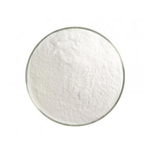
2. Processing and Microstructural Design
( Silicon Carbide Ceramics)
2.1 Sintering and Densification Methods
Silicon carbide is naturally challenging to compress as a result of its solid covalent bonding and reduced self-diffusion coefficients, needing advanced processing techniques to achieve full density without additives or with very little sintering help.
Pressureless sintering of submicron SiC powders is feasible with the enhancement of boron and carbon, which promote densification by getting rid of oxide layers and boosting solid-state diffusion.
Warm pushing applies uniaxial stress during heating, enabling complete densification at lower temperature levels (~ 1800– 2000 ° C )and creating fine-grained, high-strength parts ideal for reducing tools and wear components.
For huge or complicated shapes, reaction bonding is used, where porous carbon preforms are penetrated with molten silicon at ~ 1600 ° C, developing β-SiC in situ with marginal shrinking.
Nonetheless, residual free silicon (~ 5– 10%) remains in the microstructure, restricting high-temperature efficiency and oxidation resistance over 1300 ° C.
2.2 Additive Production and Near-Net-Shape Manufacture
Current breakthroughs in additive production (AM), particularly binder jetting and stereolithography using SiC powders or preceramic polymers, make it possible for the fabrication of intricate geometries previously unattainable with traditional techniques.
In polymer-derived ceramic (PDC) paths, fluid SiC precursors are shaped via 3D printing and after that pyrolyzed at high temperatures to produce amorphous or nanocrystalline SiC, frequently requiring more densification.
These methods reduce machining prices and material waste, making SiC extra available for aerospace, nuclear, and warmth exchanger applications where elaborate styles improve efficiency.
Post-processing actions such as chemical vapor seepage (CVI) or liquid silicon seepage (LSI) are in some cases utilized to improve density and mechanical integrity.
3. Mechanical, Thermal, and Environmental Performance
3.1 Toughness, Solidity, and Wear Resistance
Silicon carbide places among the hardest recognized materials, with a Mohs solidity of ~ 9.5 and Vickers solidity surpassing 25 Grade point average, making it extremely resistant to abrasion, erosion, and damaging.
Its flexural strength normally ranges from 300 to 600 MPa, depending upon handling technique and grain dimension, and it keeps strength at temperature levels approximately 1400 ° C in inert atmospheres.
Crack toughness, while moderate (~ 3– 4 MPa · m ¹/ TWO), is sufficient for lots of structural applications, specifically when incorporated with fiber support in ceramic matrix compounds (CMCs).
SiC-based CMCs are used in generator blades, combustor linings, and brake systems, where they offer weight savings, fuel performance, and expanded service life over metal equivalents.
Its excellent wear resistance makes SiC ideal for seals, bearings, pump parts, and ballistic armor, where durability under rough mechanical loading is important.
3.2 Thermal Conductivity and Oxidation Security
Among SiC’s most beneficial properties is its high thermal conductivity– as much as 490 W/m · K for single-crystal 4H-SiC and ~ 30– 120 W/m · K for polycrystalline kinds– surpassing that of numerous metals and allowing efficient warmth dissipation.
This home is important in power electronic devices, where SiC tools produce less waste warmth and can run at greater power thickness than silicon-based tools.
At raised temperatures in oxidizing atmospheres, SiC develops a protective silica (SiO TWO) layer that slows down further oxidation, offering excellent ecological durability approximately ~ 1600 ° C.
Nevertheless, in water vapor-rich environments, this layer can volatilize as Si(OH)₄, bring about increased degradation– a crucial challenge in gas turbine applications.
4. Advanced Applications in Power, Electronic Devices, and Aerospace
4.1 Power Electronics and Semiconductor Instruments
Silicon carbide has actually revolutionized power electronics by allowing tools such as Schottky diodes, MOSFETs, and JFETs that operate at higher voltages, frequencies, and temperatures than silicon equivalents.
These gadgets lower energy losses in electrical vehicles, renewable resource inverters, and commercial electric motor drives, adding to global power performance improvements.
The capability to run at joint temperature levels above 200 ° C permits streamlined cooling systems and enhanced system dependability.
Furthermore, SiC wafers are used as substrates for gallium nitride (GaN) epitaxy in high-electron-mobility transistors (HEMTs), incorporating the advantages of both wide-bandgap semiconductors.
4.2 Nuclear, Aerospace, and Optical Solutions
In atomic power plants, SiC is a vital element of accident-tolerant fuel cladding, where its reduced neutron absorption cross-section, radiation resistance, and high-temperature toughness boost security and efficiency.
In aerospace, SiC fiber-reinforced compounds are used in jet engines and hypersonic automobiles for their light-weight and thermal security.
Furthermore, ultra-smooth SiC mirrors are utilized precede telescopes as a result of their high stiffness-to-density proportion, thermal stability, and polishability to sub-nanometer roughness.
In recap, silicon carbide ceramics represent a cornerstone of modern-day sophisticated materials, combining outstanding mechanical, thermal, and electronic residential properties.
Via specific control of polytype, microstructure, and processing, SiC remains to allow technical breakthroughs in energy, transportation, and severe environment engineering.
5. Supplier
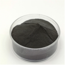
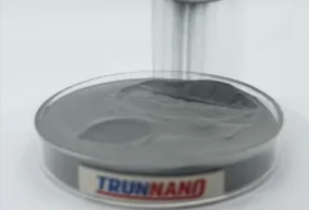
TRUNNANO is a supplier of Spherical Tungsten Powder with over 12 years of experience in nano-building energy conservation and nanotechnology development. It accepts payment via Credit Card, T/T, West Union and Paypal. Trunnano will ship the goods to customers overseas through FedEx, DHL, by air, or by sea. If you want to know more about Spherical Tungsten Powder, please feel free to contact us and send an inquiry(sales5@nanotrun.com).
Tags: silicon carbide ceramic,silicon carbide ceramic products, industry ceramic
All articles and pictures are from the Internet. If there are any copyright issues, please contact us in time to delete.
Inquiry us


