
1. Crystal Structure and Split Anisotropy
1.1 The 2H and 1T Polymorphs: Structural and Digital Duality
(Molybdenum Disulfide)
Molybdenum disulfide (MoS ₂) is a layered shift steel dichalcogenide (TMD) with a chemical formula including one molybdenum atom sandwiched between two sulfur atoms in a trigonal prismatic sychronisation, forming covalently bound S– Mo– S sheets.
These private monolayers are stacked up and down and held with each other by weak van der Waals pressures, making it possible for very easy interlayer shear and exfoliation to atomically slim two-dimensional (2D) crystals– a structural function central to its diverse useful roles.
MoS two exists in multiple polymorphic forms, one of the most thermodynamically stable being the semiconducting 2H stage (hexagonal proportion), where each layer exhibits a straight bandgap of ~ 1.8 eV in monolayer kind that transitions to an indirect bandgap (~ 1.3 eV) wholesale, a sensation essential for optoelectronic applications.
On the other hand, the metastable 1T stage (tetragonal symmetry) adopts an octahedral control and acts as a metal conductor because of electron donation from the sulfur atoms, allowing applications in electrocatalysis and conductive compounds.
Stage changes between 2H and 1T can be caused chemically, electrochemically, or through stress engineering, supplying a tunable system for creating multifunctional tools.
The capability to stabilize and pattern these stages spatially within a single flake opens paths for in-plane heterostructures with distinct electronic domain names.
1.2 Defects, Doping, and Edge States
The efficiency of MoS two in catalytic and electronic applications is extremely sensitive to atomic-scale flaws and dopants.
Inherent point flaws such as sulfur jobs function as electron contributors, boosting n-type conductivity and working as energetic sites for hydrogen advancement reactions (HER) in water splitting.
Grain borders and line problems can either hinder charge transport or create localized conductive paths, depending upon their atomic configuration.
Regulated doping with shift steels (e.g., Re, Nb) or chalcogens (e.g., Se) allows fine-tuning of the band framework, service provider concentration, and spin-orbit coupling effects.
Notably, the edges of MoS ₂ nanosheets, specifically the metal Mo-terminated (10– 10) sides, display significantly greater catalytic task than the inert basic airplane, motivating the style of nanostructured drivers with maximized edge exposure.
( Molybdenum Disulfide)
These defect-engineered systems exemplify just how atomic-level adjustment can change a naturally occurring mineral into a high-performance useful product.
2. Synthesis and Nanofabrication Techniques
2.1 Bulk and Thin-Film Manufacturing Methods
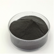
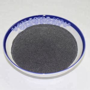
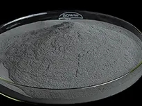
Natural molybdenite, the mineral type of MoS ₂, has been utilized for years as a solid lube, yet contemporary applications demand high-purity, structurally managed artificial types.
Chemical vapor deposition (CVD) is the dominant technique for generating large-area, high-crystallinity monolayer and few-layer MoS ₂ films on substratums such as SiO ₂/ Si, sapphire, or flexible polymers.
In CVD, molybdenum and sulfur precursors (e.g., MoO four and S powder) are vaporized at heats (700– 1000 ° C )under controlled atmospheres, allowing layer-by-layer growth with tunable domain size and orientation.
Mechanical peeling (“scotch tape method”) continues to be a standard for research-grade examples, yielding ultra-clean monolayers with marginal problems, though it does not have scalability.
Liquid-phase exfoliation, involving sonication or shear blending of mass crystals in solvents or surfactant remedies, creates colloidal diffusions of few-layer nanosheets ideal for coverings, compounds, and ink formulas.
2.2 Heterostructure Combination and Tool Patterning
The true possibility of MoS ₂ arises when integrated into vertical or side heterostructures with other 2D products such as graphene, hexagonal boron nitride (h-BN), or WSe ₂.
These van der Waals heterostructures make it possible for the style of atomically specific gadgets, including tunneling transistors, photodetectors, and light-emitting diodes (LEDs), where interlayer fee and energy transfer can be engineered.
Lithographic patterning and etching strategies allow the construction of nanoribbons, quantum dots, and field-effect transistors (FETs) with channel lengths down to tens of nanometers.
Dielectric encapsulation with h-BN safeguards MoS two from ecological degradation and reduces fee spreading, substantially boosting service provider flexibility and tool security.
These fabrication advancements are necessary for transitioning MoS two from lab interest to viable component in next-generation nanoelectronics.
3. Practical Features and Physical Mechanisms
3.1 Tribological Behavior and Strong Lubrication
Among the earliest and most long-lasting applications of MoS two is as a completely dry strong lubricating substance in extreme settings where liquid oils fall short– such as vacuum cleaner, heats, or cryogenic conditions.
The low interlayer shear strength of the van der Waals void allows very easy sliding between S– Mo– S layers, leading to a coefficient of friction as reduced as 0.03– 0.06 under optimum conditions.
Its performance is better enhanced by strong adhesion to metal surface areas and resistance to oxidation approximately ~ 350 ° C in air, beyond which MoO three formation increases wear.
MoS two is extensively used in aerospace devices, vacuum pumps, and firearm elements, typically applied as a covering through burnishing, sputtering, or composite unification into polymer matrices.
Recent research studies show that humidity can weaken lubricity by boosting interlayer bond, prompting research into hydrophobic coatings or crossbreed lubes for enhanced ecological security.
3.2 Electronic and Optoelectronic Feedback
As a direct-gap semiconductor in monolayer form, MoS ₂ displays solid light-matter communication, with absorption coefficients surpassing 10 ⁵ cm ⁻¹ and high quantum return in photoluminescence.
This makes it optimal for ultrathin photodetectors with fast feedback times and broadband sensitivity, from noticeable to near-infrared wavelengths.
Field-effect transistors based upon monolayer MoS two show on/off ratios > 10 eight and provider flexibilities as much as 500 cm TWO/ V · s in suspended samples, though substrate interactions generally limit useful worths to 1– 20 cm TWO/ V · s.
Spin-valley coupling, a consequence of strong spin-orbit interaction and damaged inversion proportion, enables valleytronics– an unique paradigm for details inscribing utilizing the valley degree of freedom in energy area.
These quantum phenomena placement MoS ₂ as a prospect for low-power reasoning, memory, and quantum computer elements.
4. Applications in Energy, Catalysis, and Arising Technologies
4.1 Electrocatalysis for Hydrogen Advancement Response (HER)
MoS ₂ has actually become an appealing non-precious choice to platinum in the hydrogen development response (HER), a crucial process in water electrolysis for eco-friendly hydrogen manufacturing.
While the basic aircraft is catalytically inert, side websites and sulfur openings display near-optimal hydrogen adsorption totally free energy (ΔG_H * ≈ 0), equivalent to Pt.
Nanostructuring techniques– such as producing up and down straightened nanosheets, defect-rich films, or drugged hybrids with Ni or Co– take full advantage of energetic website thickness and electric conductivity.
When incorporated right into electrodes with conductive sustains like carbon nanotubes or graphene, MoS ₂ attains high current thickness and long-term stability under acidic or neutral conditions.
Further enhancement is attained by maintaining the metal 1T phase, which boosts innate conductivity and exposes added energetic sites.
4.2 Flexible Electronics, Sensors, and Quantum Instruments
The mechanical flexibility, openness, and high surface-to-volume proportion of MoS ₂ make it excellent for flexible and wearable electronic devices.
Transistors, reasoning circuits, and memory devices have actually been demonstrated on plastic substrates, allowing flexible screens, wellness displays, and IoT sensors.
MoS ₂-based gas sensing units exhibit high level of sensitivity to NO ₂, NH FIVE, and H ₂ O because of bill transfer upon molecular adsorption, with action times in the sub-second variety.
In quantum modern technologies, MoS ₂ hosts local excitons and trions at cryogenic temperatures, and strain-induced pseudomagnetic areas can trap providers, enabling single-photon emitters and quantum dots.
These developments highlight MoS ₂ not just as a useful material but as a platform for discovering fundamental physics in minimized dimensions.
In summary, molybdenum disulfide exhibits the merging of timeless products scientific research and quantum engineering.
From its old role as a lubricating substance to its modern-day deployment in atomically slim electronics and energy systems, MoS ₂ remains to redefine the borders of what is feasible in nanoscale materials style.
As synthesis, characterization, and integration methods development, its influence across science and technology is positioned to expand also additionally.
5. Vendor
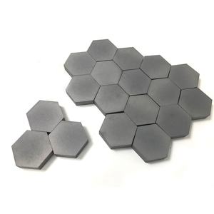
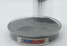
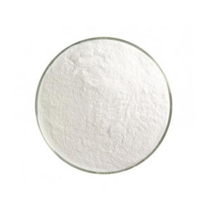
TRUNNANO is a globally recognized Molybdenum Disulfide manufacturer and supplier of compounds with more than 12 years of expertise in the highest quality nanomaterials and other chemicals. The company develops a variety of powder materials and chemicals. Provide OEM service. If you need high quality Molybdenum Disulfide, please feel free to contact us. You can click on the product to contact us.
Tags: Molybdenum Disulfide, nano molybdenum disulfide, MoS2
All articles and pictures are from the Internet. If there are any copyright issues, please contact us in time to delete.
Inquiry us


